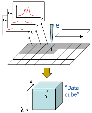
Schematic showing CL hyperspectral image acquisition
What is Cathodoluminescence?
Cathodoluminescence (CL) is the emission of light from a material under excitation by a high energy electron beam (or “cathode ray”). Various materials emit CL, including many minerals and semiconductors. In semiconductor physics, analysis of the emitted light can be used as a characterisation tool in order to probe, among other things [1]:
- the presence and type of crystal defects
- variations in composition
- changes in elastic strain
What is a hyperspectral image?
A hyperspectral image (also known as a spectrum image, or spectrum map) is an image which contains both spatial and spectral information. This can be thought of as either:
- a stack of monochromatic images each corresponding to a different wavelength band,
or equivalently: - an image in which each spatial pixel contains an entire spectrum.
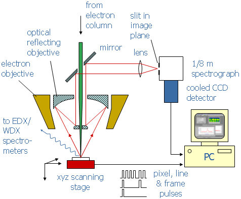
Schematic of EPMA-based CL system
CL hyperspectral image acquisition
- Measurement takes place in electron beam instrument (usually scanning electron microscope, transmission electron microscope or electron probe microanalyser)
- Electron beam scans across sample (or sample stage scans)
- At each point, acquire complete CL spectrum
- Record large 3-D (x, y, λ) dataset, or hyperspectral image
- Dataset can then be manipulated to yield different information as a function of position [2], e.g.:
- Integrated intensity (panchromatic image)
- Wavelength slice (monochromatic image)
- Peak wavelength
- Peak width
- Deconvolved peak parameters by non-linear least squares fitting of multiple peak profiles (e.g. Gaussian or Lorentzian)
- Chromaticity (i.e. calculated “real” colour)
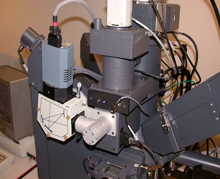
CL spectrograph mounted on Cameca SX100
EPMA-based CL hypespectral imaging system at Strathclyde
- In-house adaptation of Cameca SX100 electron probe micoanalyser (EPMA)
- Uses existing optical path and built-in reflecting objective without additional light collector
- Reduced solid angle compared with parabolic collector, offset by high efficiency, f-number matched coupling into spectrometer
- Simultaneous acquisition of elemental composition maps (using wavelength-dispersive X-ray spectrometers) and electrical information (using electron beam induced current)
- Scan dimensions from µm to cm scales
References
[1] P. R. Edwards and R. W. Martin, “Cathodoluminescence nano-characterization of semiconductors,” Semiconductor Science and Technology, vol. 26, iss. 6, p. 64005, 2011.
[Bibtex]
[Bibtex]
@Article{strathprints30546,
author = {Paul R Edwards and Robert W Martin},
journal = {Semiconductor Science and Technology},
title = {Cathodoluminescence nano-characterization of semiconductors},
year = {2011},
month = {June},
number = {6},
pages = {064005},
volume = {26},
abstract = {We give an overview of the use of cathodoluminescence (CL) in scanning electron microscopy (SEM) for the nano-scale characterization of semiconducting materials and devices. We discuss the technical aspects of the measurement, such as factors limiting the spatial resolution and design considerations for efficient collection optics. The advantages of more recent developments in the technique are outlined, including the use of the hyperspectral imaging mode and the combination of CL and other SEM-based measurements. We illustrate these points with examples from our own experience of designing and constructing CL systems and applying the technique to the characterization of III-nitride materials and nanostructures.},
keywords = {optics, condensed matter, electrical matter, magnetic matter, thin films, cathodoluminescence, ionoluminescence, Physics, Materials Chemistry, Electronic, Optical and Magnetic Materials, Electrical and Electronic Engineering, Condensed Matter Physics},
url = {http://strathprints.strath.ac.uk/30546/},
}
[2] P. R. Edwards, L. K. Jagadamma, J. Bruckbauer, C. Liu, P. Shields, D. Allsopp, T. Wang, and R. W. Martin, “High-resolution cathodoluminescence hyperspectral imaging of nitride nanostructures,” Microscopy and Microanalysis, vol. 18, iss. 6, p. 1212–1219, 2012.
[Bibtex]
[Bibtex]
@article{strathprints42421,
volume = {18},
number = {6},
month = {December},
author = {Paul R. Edwards and Lethy Krishnan Jagadamma and Jochen Bruckbauer and Chaowang Liu and Philip Shields and Duncan Allsopp and Tao Wang and Robert W. Martin},
title = {High-resolution cathodoluminescence hyperspectral imaging of nitride nanostructures},
journal = {Microscopy and Microanalysis},
pages = {1212--1219},
year = {2012},
keywords = {cathodoluminescence, hyperspectral imaging, gallium nitride, principal component analysis, multivariate statistical analysis, SEM, Physics, Instrumentation},
url = {http://strathprints.strath.ac.uk/42421/},
abstract = {Hyperspectral cathodoluminescence imaging provides spectrally and spatially resolved information on luminescent materials within a single dataset. Pushing the technique toward its ultimate nanoscale spatial limit, while at the same time spectrally dispersing the collected light before detection, increases the challenge of generating low-noise images. This article describes aspects of the instrumentation, and in particular data treatment methods, which address this problem. The methods are demonstrated by applying them to the analysis of nanoscale defect features and fabricated nanostructures in III-nitride-based materials.}
}