Researchers: Professor Robert W. Martin, Dr Carol Trager-Cowan and Dr Paul R. Edwards, Dr Jochen Bruckbauer, and Dr Douglas Cameron.
Motivation
Nitride semiconductors and their alloys are of increasing scientific interest as with improving manufacturing technology they become greatly applicable in various fields.
Nitride lighting the future
21st century light source
Light emitting diodes technology is a fast-paced field of research. Since the first compound LEDs were developed in the 50’s, efficiency and output power of the diodes improved rapidly. Howewer, as color ranges over yellow to green were available on a phosphor and aluminium basis, blue and white color LEDs were not in sight until nitride thin films got their breakthrough in the early 90’s.
LEDs on a nitride basis completed the range of primary colors and provided the first white semiconductor diodes. GaN LEDs and their alloys are currently used for specialised illumination such as stage and street lighting, displays, traffic lights or signaling.
LED illumination by Philips Lumileds
Modern LEDs beat traditional light bulbs and fluorescent lamps by magnitudes in terms of durability and efficiency. With high power diodes available in all colours, general illumination in future will increasingly rely on these devices until traditional lighting technology will be almost completely replaced by modern LEDs.
Solving the global drinking water problem
Purification of water is one of the global challenges of the 21st century. UV LEDs on a nitride basis such as AlGaN are shown to kill bacteria and they are becoming applicable in modern purification modules. As they are more efficient than conventional mercury lamps, nitride-based LEDs will greatly enhance the performance of these devices.
While germ destruction is already shown to be satisfying at low water flow-through, the main challenge is to further increase efficiency and output power of UV LEDs to increase the purified water per minute.
A big market
The LED market is certainly the most auspicious field for nitrides. Since the first commercial GaN LEDs were shipped in 1995, the market of nitride substates has grown at an average annual rate of about 50% and it is expected to even speed up its rapid hike. The market is driven by increasing demand for blue-violet lasers and ultraviolet LEDs. As new applications become available such as blu-ray and HD DVD technology, nitride-based diodes are becoming inreasingly important – they are predicted to comprise more than one-half of the LED market at 2010 (Strategies Unlimited).
A highly versatile material
Nitride – the new silicon?
Apart from optoelectronics, gallium nitride are causing a stir in the electronics department. First GaN transistors are shown to be magnitudes more powerful than transistors based on silicon and gallium arsenide. Because of their large band gap, more voltage can be applied while yielding a high current.
Whether gallium nitride are unlikely to replace silicon in computational devices, they aim for applications where high power/high frequency is needed, e.g. in mobile phones. More power leads to higher frequency and thus, increased transmission speed. And transmission speed is in high demand – the first live-streaming mobile phones are on the road.
Modern solar cells
Indium gallium nitride cover a wide energy range of radiation. They are considered to provide alternatives to multijunction solar cells as they can be tuned to cover almost the full spectrum of sunlight. Multijunction cells currently rely on different materials to achieve this range. Howewer, composing these materials is hindered by their lattice mismatch. A big advantage of Indium gallium nitrides is their high tolerance towards lattice mismatching. In theory, efficiencies up to 70% could be achieved by composing many layers of indium gallium nitrides tuned to a range of bandgaps.
Molecular sensing
Apart from detectors in the range of blue-ultraviolet as a sideline to LED development, nitride will be used in chemical detection. Due to their piezoelectric character, gallium nitride and alloys sense differences in chemical composition of a gas or liquid by responding to the surface charge induced by polar molecules at contact.
Their ability to tolerate high temperatures and pressures makes them suitable for electronic devices such as gas detectors which can be used in rough environments, e.g. oil filled equipment.
Chemical detection is increasingly applied in medicine. First GaN sensors are used to detect changes in chemical properties of small (nanolitre) samples such as concentration or cell activity. One of the main advantages of these transistor-based devices are the great tunability. The sensors can be adjusted to respond to a certain type of substrate by modifying the transistors gate area.
Research at Strathclyde
Dislocations and structure of nitrides
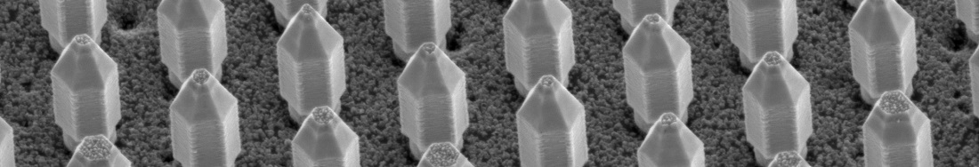
The main problem that constricts nitride-based future developments is the variable structural quality of nitride thin films because of the lattice mismatch between them and the substrates used to grow this material. Dislocation densities in GaN films can range from 108 to 1010 dislocations per square centimetre [1].
Dislocations reduce the efficiency of diodes as they act as nonradiative recombination centres. They also degrade the conductivity of the material which restricts efficiency and power of nitrides in electrical devices.
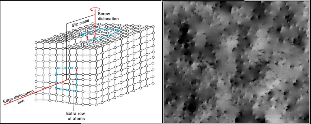
left: schematic of lattice dislocation | right: ECC image of GaN thin film
We investigate methods to reveal dislocations in nitride thin films. We map tilt, twist and strain and study their relationship to the distribution and densities of defects. Future work includes identifying the role of defects in the performance of nitride based devices on a nanometre scale and simulating dislocation contrast via dynamical electron scattering calculations.
Tuning nitrides – alloys and rare earth doping
We study the emission properties of nitride ternary alloys and their potential applications.
With GaN being ahead in the race of nitrides towards new applications, alloys allow a greater tunability, e.g. the ternary alloy InxGa1-xN emits light from violet to amber, dependent on the relative fraction of In. While changing the alloys composition offers different features, it also affects efficiency and quality of the doped material.
Another approach to tune properties of III-nitrides is the implantation of rare earth ions. These ions act as a luminescence centre, radiating at a different wavelength. The emission of the nitride host and rare earth implant mixes and results in new LED colors. Our team is currently dealing with lattice location and cathodoluminescence of rare earth doped alloys.
Characterisation methods
We are presently using attractive characterisation methods to probe the structural and luminescence properties of III-nitrides on the nanoscale:
- Wavelength-dispersive X-ray (WDX) spectroscopy
WDX uses a fixed-wavelength x-ray diffracted by the material under study and provides a quantitative measure of its composition. - Cathodoluminescence (CL) hyperspectral imaging
CL detects the luminescence spectrum of the sample which is sensitive to strain, crystallinity, defects, doping and free carrier concentration. Cathodoluminescence gives information about composition, growth and quality of the material with resolutions up to 10-20nm. We have developed a system for simultaneusly acquiring hyperspectral CL together with high-sensitivity WDX maps to correlate composition and luminescence properties [2]. For example InN fluctuations in InxGa1-xN thin films have been measured on a scale of tens of nanometres [3]. - Electron backscatter diffraction (EBSD)
EBSD, also known as ”backscatter Kikuchi diffraction”, uses electron backscattering on highly tilted samples to produce a 2-D projection of the crystal structure. We deduced that EBSD patterns acquired from a mesh of points on a sample can be used to produce maps of crystal structure with a resolution of ca. 20nm, measure orientation schanges of the order of 0.02° and strain changes of 2×10⁻⁴ in III-nitride thin films [4]. - Electron channeling contrast imaging (ECCI)
ECCI derives images of electrons channeling down the crystal planes of a tilted sample. These images reveal defects which distort the crystal planes with a resolution of tens of nanometres. We deduced that ECCI is suitable for imaging tilt, atomic steps and threading dislocations in III-nitride thin films. - Extended X-Ray absorption fine structure (EXAFS)
EXAFS allows the acquisition of information about the local environment of a specific elemental species by analysing oscillations in X-ray absorption versus photon energy. These oscillations are caused by interference of backscattered electrons with the original X-rays.
EXAFS provides complementary information to that provided by the microscopy techniques listed above, for example, the chemical bonding, coordination numbers and bond lengths. Statistical information about the first few moments of the spatial distribution of near neighbours around a targeted atomic species can be obtained (e.g. Ga in an InGaN thin film).
References
[Bibtex]
@Article{Marchand1998APL73,
author = {H. Marchand and X. H. Wu and J. P. Ibbetson and P. T. Fini and P. Kozodoy and S. Keller and J. S. Speck and S. P. DenBaars and U. K. Mishra},
title = {Microstructure of GaN laterally overgrown by metalorganic chemical vapor deposition},
journal = {Applied Physics Letters},
year = {1998},
volume = {73},
number = {6},
pages = {747-749},
abstract = {Extended defect reduction in GaN grown by lateral epitaxial overgrowth (LEO) on large-area SiO2/GaN/Al2O3 wafers by low pressure metalorganic chemical vapor deposition is characterized using transmission electron microscopy and atomic force microscopy. The laterally overgrown GaN (LEO GaN) has a rectangular cross section with smooth (0001) and {112̄0} facets. The density of mixed-character and pure edge threading dislocations in the LEO GaN (<5×106 cm−2) is reduced by at least 3–4 orders of magnitude from that of bulk GaN (~1010 cm−2). A small number of edge dislocations with line directions parallel to the basal plane are generated between the bulk-like overgrown GaN and the LEO GaN regions as well as at the intersection of adjacent merging LEO GaN stripes. The edge dislocations are most likely generated to accommodate the small misorientation between bulk-like GaN and LEO GaN regions as well as between adjacent single-crystal LEO GaN stripes.},
doi = {10.1063/1.121988}
}[Bibtex]
@Article{Martin2004PSSA201,
author = {Martin, R. W. and Edwards, P. R. and O'Donnell, K. P. and Dawson, M. D. and Jeon, C. W. and Liu, C. and Rice, G. R. and Watson, I. M.},
title = {Cathodoluminescence spectral mapping of {III}-nitride structures},
journal = {Physica Status Solidi A},
year = {2004},
volume = {201},
number = {4},
pages = {665-672},
abstract = {The application of cathodoluminescence spectral mapping to the characterisation of a range III-nitride semiconductor structures is described. Details are presented of the instrumentation developed to carry out such measurements using an electron probe micro-analyser. The spatial resolution of the luminescence data is ∼100 nm. The technique is enhanced by the ability to simultaneously perform X-ray microanalysis and electron imaging. Results are presented from epitaxially laterally overgrown GaN and InGaN/GaN structures using both single-layer SiO2 and multilayer SiO2/ZrO2 masks. Effects of strain and microcavity formation are resolved. Application of the technique to InGaN epilayers shows spatially-dependent shifts in the peak wavelength of the luminescence spectrum which correlate directly with microscopic variations in the indium content. Regions emitting at lower energy and with decreased intensity are shown to have higher InN contents, mirroring equivalent macroscopic observations. Finally the spectral mapping technique is used to analyse the luminescence from micron-scale selectively grown III-N pyramids, indicating possible formation of quantum dots at the sharp tips.},
doi = {10.1002/pssa.200304089}
}[Bibtex]
@Article{Edwards2003PSSC0,
author = {Edwards, P. R. and Martin, R. W. and O'Donnell, K. P. and Watson, I. M.},
title = {Simultaneous composition mapping and hyperspectral cathodoluminescence imaging of {InGaN} epilayers},
journal = {Physica Status Solidi C},
year = {2003},
volume = {0},
number = {7},
pages = {2474-2477},
abstract = {Gallium nitride based structures have been characterised using the novel approach of simultaneous wavelength-dispersive X-ray microanalysis and cathodoluminescence spectral mapping (or hyperspectral imaging). Details are presented of the instrumentation developed to carry out such measurements. Application of the technique to MOVPE-grown indium gallium nitride epilayers shows microscopic variations in the indium content, which correlate directly with spatially-dependent shifts observed in the peak wavelength of the luminescence spectrum. Regions of higher indium content are shown to emit at lower energy and with decreased intensity, mirroring equivalent macroscopic observations.},
doi = {10.1002/pssc.200303510},
owner = {Paul},
timestamp = {2012.05.15}
}[Bibtex]
@Article{Trager-Cowan2006MST22,
author = {C. Trager-Cowan and F. Sweeney and A. Winkelmann and A. J. Wilkinson and P. W. Trimby and A. P. Day and A. Gholinia and N. H. Schmidt and P. J. Parbrook and I. M. Watson},
title = {Characterisation of nitride thin films by electron backscatter diffraction and electron channelling contrast imaging},
journal = {Materials Science and Technology},
year = {2006},
volume = {22},
number = {11},
pages = {1352-1358},
abstract = {AbstractIn the present paper the authors describe the use of electron backscatter diffraction (EBSD) mapping and electron channelling contrast imaging (in the scanning electron microscope) to study tilt, strain, atomic steps and dislocations in epitaxial GaN thin films. Results from epitaxial GaN thin films and from a just coalesced epitaxial laterally overgrown GaN thin film are shown. From the results it is deduced that EBSD may be used to measure orientation changes of the order of 0·02° and strain changes of order 2 × 10⁻⁴ in GaN thin films. It is also demonstrated that channelling contrast in electron channelling contrast images may be used to image tilt, atomic steps and threading dislocations in GaN thin films. In addition the authors will consider the results of the first many-beam dynamical simulations of EBSD patterns from GaN thin films, in which the intensity distributions in the experimental patterns are accurately reproduced.},
doi = {10.1179/174328406X130957}
}
Further Reading
- Fred Schubert, "Light-emitting diodes hit the centenary milestone", Compound Semiconductor, Oct 15, 2007.