 All 4th year undergraduate students in the Department will undertake a year-long research project (PH450), and MSci students will continue this into their 5th year (PH550). Students can also sometimes be funded to undertake additional projects during the summer.
The Semiconductor Spectroscopy and Devices group offers theoretical and experimental projects in a range of different research areas, such as:
- Luminscence spectroscopy of semiconductors
- Scanning electron microscopy techniques
- Crystal defect physics
- Group III nitride optoelectronic devices
- Gallium oxide UV detectors
- Experimental quantum nanoscience
- G. Naresh-Kumar, H. Macintyre, S. Shanthi, P. R. Edwards, R. W. Martin, K. Daivasigamani, K. Sasaki, and A. Kuramata, “Origin of red emission in β-Ga₂O₃ analysed by cathodoluminescence and photoluminescence spectroscopy,” Physica Status Solidi B, 2020.
[BibTeX] [Abstract] [Download PDF]
The spectroscopic techniques of cathodoluminescence and photoluminescence are used to study the origin of red emission in β-Ga₂O₃ grown using the edge-defined film-fed grown (EFG) method and hydride vapor phase epitaxy. Room temperature cathodoluminescence shows red emission peaks from samples doped with Fe, Sn, and Si and from unintentionally doped samples. Narrow emission lines around 690 nm are seen strongly in the Fe and unintentionally doped samples. Temperature-dependent photoluminescence analysis of the two prominent red emission lines reveals properties similar to the R lines in sapphire for all the samples, but with different level of existence. These lines are attributed to Cr³⁺ ionic transitions rather than to Fe³⁺, as reported previously. The most likely origin of the unintentional Cr incorporation is the source material used in the EFG method.
@Article{strathprints74145,
author = {Gunasekar Naresh-Kumar and Hazel Macintyre and Shanthi Shanthi and Paul R. Edwards and Robert W. Martin and Krishnamurthy Daivasigamani and Kohei Sasaki and Akito Kuramata},
journal = {Physica Status Solidi B},
title = {Origin of red emission in {β-Ga₂O₃} analysed by cathodoluminescence and photoluminescence spectroscopy},
year = {2020},
month = {October},
abstract = {The spectroscopic techniques of cathodoluminescence and photoluminescence are used to study the origin of red emission in β-Ga₂O₃ grown using the edge-defined film-fed grown (EFG) method and hydride vapor phase epitaxy. Room temperature cathodoluminescence shows red emission peaks from samples doped with Fe, Sn, and Si and from unintentionally doped samples. Narrow emission lines around 690 nm are seen strongly in the Fe and unintentionally doped samples. Temperature-dependent photoluminescence analysis of the two prominent red emission lines reveals properties similar to the R lines in sapphire for all the samples, but with different level of existence. These lines are attributed to Cr³⁺ ionic transitions rather than to Fe³⁺, as reported previously. The most likely origin of the unintentional Cr incorporation is the source material used in the EFG method.},
keywords = {spectroscopy methods, gallium oxide, scanning electron microscope (SEM), cathodoluminescence, photoluminescence, Physics, Electronic, Optical and Magnetic Materials, Condensed Matter Physics},
url = {https://strathprints.strath.ac.uk/74145/},
}
- D. Cameron, K. P. O’Donnell, P. R. Edwards, M. Peres, K. Lorenz, M. J. Kappers, and M. Boćkowski, “Acceptor state anchoring in gallium nitride,” Applied Physics Letters, vol. 116, p. 102105, 2020. doi:10.1063/1.5142168
[BibTeX] [Abstract] [Download PDF]
The dual nature of the magnesium acceptor in gallium nitride results in dynamic defect complexes. Europium spectator ions reveal switching between two spectrally unique metastable centres, each corresponding to a particular acceptor state. By ion co-implantation of europium and oxygen into GaN(Mg), we produce, in addition, an anchored state system. In doing so we create an abundance of previously unidentified stable centres which we denote as “Eu0(Ox)”. We introduce a microscopic model for these centres with oxygen substituting for nitrogen in the bridging site.
@Article{strathprints71643,
author = {D. Cameron and K. P. O'Donnell and P. R. Edwards and M. Peres and K. Lorenz and M. J. Kappers and M. Bo{\'c}kowski},
journal = {Applied Physics Letters},
title = {Acceptor state anchoring in gallium nitride},
year = {2020},
month = {February},
pages = {102105},
volume = {116},
abstract = {The dual nature of the magnesium acceptor in gallium nitride results in dynamic defect complexes. Europium spectator ions reveal switching between two spectrally unique metastable centres, each corresponding to a particular acceptor state. By ion co-implantation of europium and oxygen into GaN(Mg), we produce, in addition, an anchored state system. In doing so we create an abundance of previously unidentified stable centres which we denote as "Eu0(Ox)". We introduce a microscopic model for these centres with oxygen substituting for nitrogen in the bridging site.},
doi = {10.1063/1.5142168},
keywords = {rare earth (RE) ions, europium, gallium nitride, Physics, Electronic, Optical and Magnetic Materials, Condensed Matter Physics},
url = {https://strathprints.strath.ac.uk/71643/},
}
- C. Trager-Cowan, A. Alasmari, W. Avis, J. Bruckbauer, P. R. Edwards, G. Ferenczi, B. Hourahine, A. Kotzai, S. Kraeusel, G. Kusch, R. W. Martin, R. McDermott, N. Gunasekar, M. Nouf-Allehiani, E. Pascal, D. Thomson, S. Vespucci, M. D. Smith, P. J. Parbrook, J. Enslin, F. Mehnke, C. Kuhn, T. Wernicke, M. Kneissl, S. Hagedorn, A. Knauer, S. Walde, M. Weyers, P. Coulon, P. Shields, J. Bai, Y. Gong, L. Jiu, Y. Zhang, R. Smith, T. Wang, and A. Winkelmann, “Structural and luminescence imaging and characterisation of semiconductors in the scanning electron microscope,” Semiconductor Science and Technology, vol. 35, p. 54001, 2020. doi:10.1088/1361-6641/ab75a5
[BibTeX] [Abstract] [Download PDF]
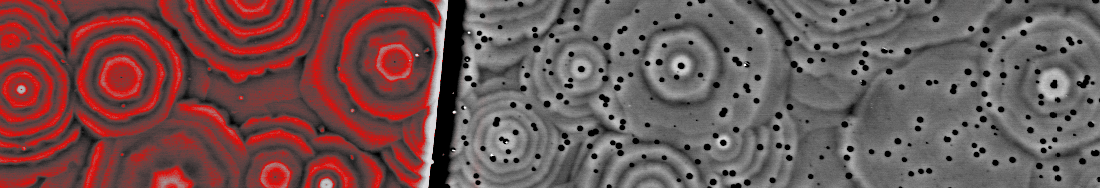
The scanning electron microscopy techniques of electron backscatter diffraction (EBSD), electron channelling contrast imaging (ECCI) and hyperspectral cathodoluminescence imaging (CL) provide complementary information on the structural and luminescence properties of materials rapidly and non-destructively, with a spatial resolution of tens of nanometres. EBSD provides crystal orientation, crystal phase and strain analysis, whilst ECCI is used to determine the planar distribution of extended defects over a large area of a given sample. CL reveals the influence of crystal structure, composition and strain on intrinsic luminescence and/or reveals defect-related luminescence. Dark features are also observed in CL images where carrier recombination at defects is non-radiative. The combination of these techniques is a powerful approach to clarifying the role of crystallography and extended defects on a materials’ light emission properties. Here we describe the EBSD, ECCI and CL techniques and illustrate their use for investigating the structural and light emitting properties of UV-emitting nitride semiconductor structures. We discuss our investigations of the type, density and distribution of defects in GaN, AlN and AlGaN thin films and also discuss the determination of the polarity of GaN nanowires.
@Article{strathprints71512,
author = {Carol Trager-Cowan and Aeshah Alasmari and William Avis and Jochen Bruckbauer and Paul R. Edwards and Gergely Ferenczi and Benjamin Hourahine and Almpes Kotzai and Simon Kraeusel and Gunnar Kusch and Robert W. Martin and Ryan McDermott and Naresh Gunasekar and M. Nouf-Allehiani and Elena Pascal and David Thomson and Stefano Vespucci and Matthew David Smith and Peter J. Parbrook and Johannes Enslin and Frank Mehnke and Christian Kuhn and Tim Wernicke and Michael Kneissl and Sylvia Hagedorn and Arne Knauer and Sebastian Walde and Markus Weyers and Pierre-Marie Coulon and Philip Shields and J. Bai and Y. Gong and Ling Jiu and Y. Zhang and Richard Smith and Tao Wang and Aimo Winkelmann},
journal = {Semiconductor Science and Technology},
title = {Structural and luminescence imaging and characterisation of semiconductors in the scanning electron microscope},
year = {2020},
month = {February},
pages = {054001},
volume = {35},
abstract = {The scanning electron microscopy techniques of electron backscatter diffraction (EBSD), electron channelling contrast imaging (ECCI) and hyperspectral cathodoluminescence imaging (CL) provide complementary information on the structural and luminescence properties of materials rapidly and non-destructively, with a spatial resolution of tens of nanometres. EBSD provides crystal orientation, crystal phase and strain analysis, whilst ECCI is used to determine the planar distribution of extended defects over a large area of a given sample. CL reveals the influence of crystal structure, composition and strain on intrinsic luminescence and/or reveals defect-related luminescence. Dark features are also observed in CL images where carrier recombination at defects is non-radiative. The combination of these techniques is a powerful approach to clarifying the role of crystallography and extended defects on a materials' light emission properties. Here we describe the EBSD, ECCI and CL techniques and illustrate their use for investigating the structural and light emitting properties of UV-emitting nitride semiconductor structures. We discuss our investigations of the type, density and distribution of defects in GaN, AlN and AlGaN thin films and also discuss the determination of the polarity of GaN nanowires.},
doi = {10.1088/1361-6641/ab75a5},
keywords = {EBSD, nitride, scanning electron microscopy, Physics, Electronic, Optical and Magnetic Materials, Electrical and Electronic Engineering, Condensed Matter Physics},
url = {https://strathprints.strath.ac.uk/71512/},
}
- P. R. Edwards, K. P. O’Donnell, A. K. Singh, D. Cameron, K. Lorenz, M. Yamaga, J. H. Leach, M. J. Kappers, and M. Boćkowski, “Hysteretic photochromic switching (HPS) in doubly doped GaN(Mg):Eu–a summary of recent results,” Materials, vol. 11, iss. 10, p. 1800, 2018.
[BibTeX] [Abstract] [Download PDF]
Europium is the most-studied and least-well-understood rare earth ion (REI) dopant in GaN. While attempting to increase the efficiency of red GaN light-emitting diodes (LEDs) by implanting Eu+ into p-type GaN templates, the Strathclyde University group, in collaboration with IST Lisbon and Unipress Warsaw, discovered hysteretic photochromic switching (HPS) in the photoluminescence spectrum of doubly doped GaN(Mg):Eu. Our recent work, summarised in this contribution, has used time-, temperature- and light-induced changes in the Eu intra-4f shell emission spectrum to deduce the microscopic nature of the Mg-Eu defects that form in this material. As well as shedding light on the Mg acceptor in GaN, we propose a possible role for these emission centres in quantum information and computing.
@Article{strathprints65532,
author = {Paul R. Edwards and Kevin P. O'Donnell and Akhilesh K. Singh and Douglas Cameron and Katharina Lorenz and Mitsuo Yamaga and Jacob H. Leach and Menno J. Kappers and Michal Bo{\'c}kowski},
title = {Hysteretic photochromic switching (HPS) in doubly doped GaN(Mg):Eu{--}a summary of recent results},
journal = {Materials},
year = {2018},
volume = {11},
number = {10},
pages = {1800},
month = {September},
abstract = {Europium is the most-studied and least-well-understood rare earth ion (REI) dopant in GaN. While attempting to increase the efficiency of red GaN light-emitting diodes (LEDs) by implanting Eu+ into p-type GaN templates, the Strathclyde University group, in collaboration with IST Lisbon and Unipress Warsaw, discovered hysteretic photochromic switching (HPS) in the photoluminescence spectrum of doubly doped GaN(Mg):Eu. Our recent work, summarised in this contribution, has used time-, temperature- and light-induced changes in the Eu intra-4f shell emission spectrum to deduce the microscopic nature of the Mg-Eu defects that form in this material. As well as shedding light on the Mg acceptor in GaN, we propose a possible role for these emission centres in quantum information and computing.},
keywords = {gallium nitride, rare earth ions, europium, photoluminescence, photochromism, qubit, Physics, Materials Science(all), Physics and Astronomy(all)},
url = {https://strathprints.strath.ac.uk/65532/}
}
- A. K. Singh, K. P. O’Donnell, P. R. Edwards, D. Cameron, K. Lorenz, M. J. Kappers, M. Boćkowski, M. Yamaga, and R. Prakash, “Luminescence of Eu³⁺ in GaN(Mg, Eu) : transitions from the ⁵D₁ level,” Applied Physics Letters, vol. 111, p. 241105, 2017.
[BibTeX] [Abstract] [Download PDF]
Eu-doped GaN(Mg) exemplifies hysteretic photochromic switching between two configurations, Eu0 and Eu1(Mg), of the same photoluminescent defect. Using above bandgap excitation, we studied the temperature dependence of photoluminescence (TDPL) of transitions from the excited ⁵D₁ level of Eu³⁺ for both configurations of this defect. During sample cooling, ⁵D₁→⁷F₀,₁,₂ transitions of Eu0 manifest themselves at temperatures below ~200 K, while those of Eu1(Mg) appear only during switching. The observed line positions verify crystal field energies of the ⁷F₀,₁,₂ levels. TDPL profiles of ⁵D₁→⁷F₁ and ⁵D₀→7FJ transitions of Eu0 show an onset of observable emission from the ⁵D₁ level coincident with the previously observed, but hitherto unexplained, decrease in the intensity of its ⁵D₀→⁷FJ emission on cooling below 200 K. Hence the ⁵D₀→⁷FJ TDPL anomaly signals a back-up of ⁵D₁ population due to a reduction in phonon-assisted relaxation between ⁵D₁ and ⁵D₀ levels at lower temperatures. We discuss this surprising result in the light of temperature-dependent transient luminescence measurements of Eu0.
@Article{strathprints62516,
author = {A.K. Singh and K.P. O'Donnell and P.R. Edwards and D. Cameron and K. Lorenz and M.J. Kappers and M. Bo{\'c}kowski and M. Yamaga and R. Prakash},
title = {Luminescence of Eu³⁺ in GaN(Mg, Eu) : transitions from the ⁵D₁ level},
journal = {Applied Physics Letters},
year = {2017},
volume = {111},
pages = {241105},
month = {November},
abstract = {Eu-doped GaN(Mg) exemplifies hysteretic photochromic switching between two configurations, Eu0 and Eu1(Mg), of the same photoluminescent defect. Using above bandgap excitation, we studied the temperature dependence of photoluminescence (TDPL) of transitions from the excited ⁵D₁ level of Eu³⁺ for both configurations of this defect. During sample cooling, ⁵D₁→⁷F₀,₁,₂ transitions of Eu0 manifest themselves at temperatures below ~200 K, while those of Eu1(Mg) appear only during switching. The observed line positions verify crystal field energies of the ⁷F₀,₁,₂ levels. TDPL profiles of ⁵D₁→⁷F₁ and ⁵D₀→7FJ transitions of Eu0 show an onset of observable emission from the ⁵D₁ level coincident with the previously observed, but hitherto unexplained, decrease in the intensity of its ⁵D₀→⁷FJ emission on cooling below 200 K. Hence the ⁵D₀→⁷FJ TDPL anomaly signals a back-up of ⁵D₁ population due to a reduction in phonon-assisted relaxation between ⁵D₁ and ⁵D₀ levels at lower temperatures. We discuss this surprising result in the light of temperature-dependent transient luminescence measurements of Eu0.},
keywords = {photoluminescence, bandgap, temperature, Physics, Physics and Astronomy(all)},
url = {https://strathprints.strath.ac.uk/62516/}
}
- J. Bruckbauer, C. Brasser, N. J. Findlay, P. R. Edwards, D. J. Wallis, P. J. Skabara, and R. W. Martin, “Colour tuning in white hybrid inorganic/organic light-emitting diodes,” Journal of Physics D: Applied Physics, vol. 49, iss. 40, p. 405103, 2016.
[BibTeX] [Abstract] [Download PDF]
White hybrid inorganic/organic light-emitting diodes (LEDs) were fabricated by combining a novel organic colour converter with a blue inorganic LED. An organic small molecule was specifically synthesised to act as down-converter. The characteristics of the white colour were controlled by changing the concentration of the organic molecule based on the BODIPY unit, which was embedded in a transparent matrix, and volume of the molecule and encapsulant mixture. The concentration has a critical effect on the conversion efficiency, i.e. how much of the absorbed blue light is converted into yellow light. With increasing concentration the conversion efficiency decreases. This quenching effect is due to aggregation of the organic molecule at higher concentrations. Increasing the deposited amount of the converter does not increase the yellow emission despite more blue light being absorbed. Degradation of the organic converter was also observed during a period of 15 months from LED fabrication. Angular-dependent measurements revealed slight deviation from a Lambertian profile for the blue and yellow emission peaks leading to a small change in “whiteness” with emission angle. Warm white and cool white light with correlated colour temperatures of 2770 K and 7680 K, respectively, were achieved using different concentrations of the converter molecule. Although further work is needed to improve the lifetime and poor colour rendering, these hybrid LEDs show promising results as an alternative approach for generating white LEDs compared with phosphor-based white LEDs.
@Article{strathprints57454,
author = {Jochen Bruckbauer and Catherine Brasser and Neil J. Findlay and Paul R. Edwards and David J. Wallis and Peter J. Skabara and Robert W. Martin},
title = {Colour tuning in white hybrid inorganic/organic light-emitting diodes},
journal = {Journal of Physics D: Applied Physics},
year = {2016},
volume = {49},
number = {40},
pages = {405103},
month = {September},
abstract = {White hybrid inorganic/organic light-emitting diodes (LEDs) were fabricated by combining a novel organic colour converter with a blue inorganic LED. An organic small molecule was specifically synthesised to act as down-converter. The characteristics of the white colour were controlled by changing the concentration of the organic molecule based on the BODIPY unit, which was embedded in a transparent matrix, and volume of the molecule and encapsulant mixture. The concentration has a critical effect on the conversion efficiency, i.e. how much of the absorbed blue light is converted into yellow light. With increasing concentration the conversion efficiency decreases. This quenching effect is due to aggregation of the organic molecule at higher concentrations. Increasing the deposited amount of the converter does not increase the yellow emission despite more blue light being absorbed. Degradation of the organic converter was also observed during a period of 15 months from LED fabrication. Angular-dependent measurements revealed slight deviation from a Lambertian profile for the blue and yellow emission peaks leading to a small change in "whiteness" with emission angle. Warm white and cool white light with correlated colour temperatures of 2770 K and 7680 K, respectively, were achieved using different concentrations of the converter molecule. Although further work is needed to improve the lifetime and poor colour rendering, these hybrid LEDs show promising results as an alternative approach for generating white LEDs compared with phosphor-based white LEDs.},
keywords = {light-emitting diode, energy efficiencey, organic converter, colour converter, hybrid white LED, inorganic blue LED, Optics. Light, Atomic and Molecular Physics, and Optics, Surfaces, Coatings and Films, Energy Engineering and Power Technology},
url = {http://strathprints.strath.ac.uk/57454/}
}
- F. Luckert, D. I. Hamilton, M. V. Yakushev, N. S. Beattie, G. Zoppi, M. Moynihan, I. Forbes, A. V. Karotki, A. V. Mudryi, M. Grossberg, J. Krustok, and R. W. Martin, “Optical properties of high quality Cu₂ZnSnSe₄ thin films,” Applied Physics Letters, vol. 99, iss. 6, p. 62104, 2011.
[BibTeX] [Abstract] [Download PDF]
Cu2ZnSnSe4 thin films, fabricated on bare or molybdenum coated glass substrates by magnetron sputtering and selenisation, were studied by a range of techniques. Photoluminescence spectra reveal an excitonic peak and two phonon replicas of a donor-acceptor pair (DAP) recombination. Its acceptor and donor ionisation energies are 27 and 7 meV, respectively. This demonstrates that high-quality Cu2ZnSnSe4 thin films can be fabricated. An experimental value for the longitudinal optical phonon energy of 28 meV was estimated. The band gap energy of 1.01 eV at room temperature was determined using optical absorption spectra.
@Article{strathprints34031,
author = {F. Luckert and D. I. Hamilton and M. V. Yakushev and N. S. Beattie and G. Zoppi and M. Moynihan and I. Forbes and A. V. Karotki and A. V. Mudryi and M. Grossberg and J. Krustok and R. W. Martin},
title = {Optical properties of high quality Cu₂ZnSnSe₄ thin films},
journal = {Applied Physics Letters},
year = {2011},
volume = {99},
number = {6},
pages = {062104},
month = {August},
abstract = {Cu2ZnSnSe4 thin films, fabricated on bare or molybdenum coated glass substrates by magnetron sputtering and selenisation, were studied by a range of techniques. Photoluminescence spectra reveal an excitonic peak and two phonon replicas of a donor-acceptor pair (DAP) recombination. Its acceptor and donor ionisation energies are 27 and 7 meV, respectively. This demonstrates that high-quality Cu2ZnSnSe4 thin films can be fabricated. An experimental value for the longitudinal optical phonon energy of 28 meV was estimated. The band gap energy of 1.01 eV at room temperature was determined using optical absorption spectra.},
keywords = {photoluminescence, selenisation, dependence, energy, copper compounds, excitons, phonons, photoionisation, Raman spectra, semiconductor thin films, sputter deposition, tin compounds, zinc compounds, TIC - Bionanotechnology, Optics. Light, Physics and Astronomy (miscellaneous)},
url = {http://strathprints.strath.ac.uk/34031/}
}
- R. W. Martin, P. R. Edwards, K. P. O’Donnell, E. G. Mackay, and I. M. Watson, “Microcomposition and luminescence of InGaN emitters,” Physica Status Solidi A, vol. 192, iss. 1, p. 117–123, 2002.
[BibTeX] [Abstract] [Download PDF]
Using wavelength dispersive X-ray (WDX) spectrometers on an electron probe micro-analyser (EPMA) the indium content of a number of homogeneous and inhomogeneous InGaN epitaxial layers has been accurately mapped. The addition of a spectrometer and silicon CCD array to the light microscope, which shares the same focus as the electron microscope, enables cathodoluminescence spectra to be collected from exactly the same spot as sampled by the WDX spectrometers. As a result the dependencies of the luminescence energy and linewidth on the local indium nitride fraction can be investigated with greater confidence than in earlier reports, where separate measurements of luminescence and composition were required. Samples studied have indium nitride fractions ranging from {\ensuremath{<}}0.01 to approximately 0.25, corresponding to luminescence peaks covering the ultraviolet, blue and green regions of the spectrum. A linear dependence of luminescence peak energy on indium fraction is demonstrated and the linewidth variation plotted. Secondary electron images recorded in the EPMA reveal a wide range of topographies, varying from coalesced micrometre-scale hexagonal crystallites to densely packed layers.
@article{strathprints23331,
volume = {192},
number = {1},
month = {July},
author = {R.W. Martin and P.R. Edwards and K.P. O'Donnell and E.G. Mackay and I.M. Watson},
title = {Microcomposition and luminescence of InGaN emitters},
journal = {Physica Status Solidi A},
pages = {117--123},
year = {2002},
keywords = {quantum wells, epilayers, growth, diodes, Physics, Materials Chemistry, Surfaces, Coatings and Films, Surfaces and Interfaces, Electronic, Optical and Magnetic Materials, Electrical and Electronic Engineering, Condensed Matter Physics},
url = {http://strathprints.strath.ac.uk/23331/},
abstract = {Using wavelength dispersive X-ray (WDX) spectrometers on an electron probe micro-analyser (EPMA) the indium content of a number of homogeneous and inhomogeneous InGaN epitaxial layers has been accurately mapped. The addition of a spectrometer and silicon CCD array to the light microscope, which shares the same focus as the electron microscope, enables cathodoluminescence spectra to be collected from exactly the same spot as sampled by the WDX spectrometers. As a result the dependencies of the luminescence energy and linewidth on the local indium nitride fraction can be investigated with greater confidence than in earlier reports, where separate measurements of luminescence and composition were required. Samples studied have indium nitride fractions ranging from {\ensuremath{<}}0.01 to approximately 0.25, corresponding to luminescence peaks covering the ultraviolet, blue and green regions of the spectrum. A linear dependence of luminescence peak energy on indium fraction is demonstrated and the linewidth variation plotted. Secondary electron images recorded in the EPMA reveal a wide range of topographies, varying from coalesced micrometre-scale hexagonal crystallites to densely packed layers.}
}